Efficient product development hinges on one critical factor: cost. For engineers, technicians, and electronics designers, prototyping printed circuit boards (PCBs) often becomes a costly and time-intensive stage in the development process. Therefore, focusing on PCB prototyping cost reduction is essential. Identifying issues after manufacturing, for example, can lead to spiraling expenses, redesign efforts, and delays in delivering the final product.
This is where PCB Sherlock Analysis comes into play—a game-changing tool designed to predict failures and optimize designs well before the first prototype is developed. At Relteck, innovation is at the heart of our mission, and we are proud to help engineers cut prototyping costs by up to 50%.
If you’re ready to revolutionize the way you approach PCB design, this post will guide you through what PCB Sherlock Analysis is, how it drives cost savings, and why it’s an invaluable tool for engineers and designers alike.
What Is PCB Sherlock Analysis and How Does It Work?
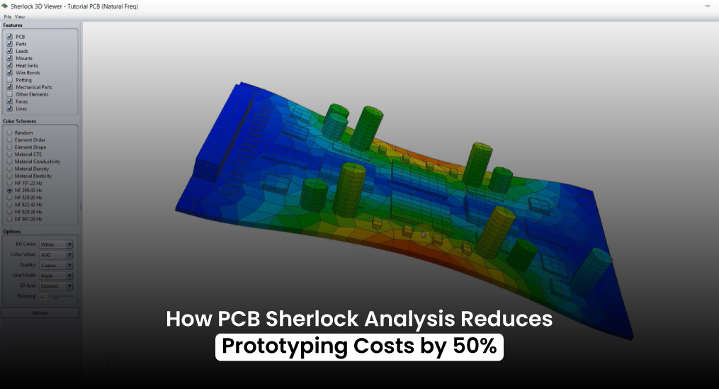
Before we delve into how this tool slashes costs, let’s first break down what PCB Sherlock Analysis is. Developed as a cutting-edge failure analysis tool, it seamlessly combines advanced simulation technology with predictive algorithms. As a result, the system is able to effectively evaluate a PCB’s design durability and reliability.
PCB Sherlock reads and analyzes design files, such as Gerber files, schematics, and CAD models, to simulate:
- Material stresses under operational loads.
- Thermal dynamics that can lead to overheating.
- Component reliability based on placement and usage conditions.
The technology incorporates industry-standard failure prediction methods, such as Mean Time Between Failures (MTBF), to calculate the lifespan and weaknesses of the board. By predicting potential issues before manufacturing, it enables engineers to refine their designs upfront, reducing costly rework in the prototyping stage.
Key Features of PCB Sherlock for PCB Prototyping Cost Reduction:
- Design Flaw Detection: It identifies structural weaknesses, thermal concerns, and material mismatches.
- Reliability Predictions: Sherlock provides reports estimating the lifespan of the PCB under different stressors.
- Automated Analysis: The system integrates seamlessly with existing CAD tools, saving engineers time.
With PCB Sherlock, design teams can easily simulate real-world conditions. As a result, they can ensure that faulty designs are caught early in the process, preventing costly errors and delays.
How PCB Sherlock Analysis Reduces Prototyping Costs

There’s no question that prototyping is an essential part of PCB development. However, traditional prototyping often involves multiple iterations to refine designs, with each iteration adding to the overall cost. Consequently, this is where PCB failure analysis costs can quickly skyrocket.
PCB Sherlock Analysis addresses this challenge by shifting the problem-solving process to the earliest stage of development. As a result, manufacturers often see up to a 50% reduction in prototyping costs. This is because the tool:
1. Identifies Flaws Early, Reducing PCB Prototyping Costs
By pinpointing issues like weak solder joints, thermal stress points, and insufficient design margins, Sherlock effectively eliminates the need for extensive physical testing. As a result, without PCB Sherlock Analysis, these issues may only surface once the initial prototypes are tested, ultimately necessitating costly redesigns.
2. Improves MTBF, Contributing to PCB Prototyping Cost Reduction
For semiconductors and electronics, the MTBF formula is integral to determining reliability. Moreover, PCB Sherlock enhances the accuracy of MTBF predictions by factoring in operating environments, materials, and stressors. As a result, this ensures components meet their expected lifespan, thereby reducing the costs associated with premature product failure.
3. Saves Prototyping Time, Driving PCB Prototyping Cost Reduction
Time is money, especially in the fast-paced electronics industry. Fortunately, with PCB Sherlock, the typical iterative prototyping process is significantly reduced, as engineers receive actionable insights after their initial design. As a result, this can easily shave weeks off the production timeline.
Real-World Example: PCB Prototyping Cost Reduction in Action:
A global semiconductor firm partnered with Relteck to integrate PCB Sherlock Analysis into its design process. By using it to optimize PCB layouts and identify solder fatigue issues in their initial design phase, they eliminated two prototyping cycles, saving $75,000 in development costs and reducing their time-to-market by nearly a month.
Why Engineers Love PCB Sherlock for PCB Prototyping Cost Reduction
Whether you’re an electrical engineer, a technician, or a semiconductor designer, PCB Sherlock Analysis offers solutions that are specifically tailored to your workflow. In fact, here’s how this tool benefits professionals across the industry:
Engineers
- Enhanced Precision: Gain insights into stress points and thermal vulnerabilities to create robust PCBs from the outset.
- Seamless Integration: With CAD compatibility, engineers can easily import design files directly into Sherlock for analysis.
Electronics Designers
- Better Aesthetics and Functionality: By simulating component placement, designers can ensure boards are not only effective but also meet space constraints.
- Reliability Confidence: Understanding the lifetime of a board gives designers the peace of mind that their creations are long-lasting.
Technicians
- Simplified Debugging: Sherlock’s extensive reports make it easier for technicians to troubleshoot and address issues immediately.
- Reduced Testing Load: Proactive analysis means less reliance on exhaustive physical testing, freeing technicians to focus on optimizing outcomes.
Semiconductor Engineers
- Lifetime Validation: Simulate and confirm the reliability of semiconductors under various operating conditions.
- Cost Efficiency: By reducing the chance of failure, Sherlock streamlines the entire product development lifecycle.
Investing in a tool like PCB Sherlock Analysis doesn’t just save money upfront; in fact, it sets the foundation for long-term success in competitive markets.
Building Stronger Designs with Relteck
At Relteck, we are committed to empowering engineers and designers to optimize their workflows and create PCB designs that not only meet but exceed expectations. By utilizing tools like PCB Sherlock Analysis, you can, in turn, minimize prototyping expenses, enhance reliability, and ultimately accelerate your path to innovation. Moreover, this approach ensures that your designs are more efficient and cost-effective, leading to higher-quality outcomes.
Key Takeaways:
- PCB prototyping can be costly, but tools like PCB Sherlock help reduce expenses by 50%.
- By identifying potential failures early, Sherlock saves time and money while improving product reliability.
- Engineers, designers, and technicians benefit directly from seamless integration and actionable insights.
Are you ready to revolutionize your approach to PCB design? Contact Relteck today to learn more about incorporating PCB Sherlock Analysis into your processes. Together, we’ll take your designs from concept to perfection.